Originally published by DeepTech
Edited and translated by LinkZill
In early June, Anthropic called for a global slowdown in AI development. Its concern was not simply that AI capabilities are advancing rapidly, but that alignment research, supply chains, and market mechanisms are failing to keep pace.
This imbalance is particularly evident in AI for Science (AI4S). AI can dramatically accelerate scientific discovery, but it cannot automatically validate what it discovers. The question, therefore, is not only whether frontier AI should slow down, but how experimental validation, engineering integration, and industrialization can catch up.
Materials science illustrates the challenge. In 2023, Google DeepMind predicted 2.2 million new crystal structures, including approximately 380,000 considered potentially synthesizable. Yet only around 700 have been synthesized worldwide over the past three years.
Even synthesis is only the beginning. A new material must still be tested for array-level performance, uniformity, stability, manufacturability, and suitability for real-world systems before its commercial potential can be established.
Who Will Validate the Materials Designed by AI?
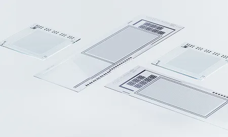
Thin-film transistors (TFTs) provide precise, independent electrical control over millions of pixels in modern displays. Their inherent scalability, density, and array-based architecture also make them well suited to the validation of emerging materials and devices.
Mainland China accounts for approximately 80% of global TFT production capacity and is supported by a mature industrial supply chain. Companies capable of redirecting these capabilities toward new applications therefore hold a significant structural advantage.
LinkZill is one of the leading companies in this field.
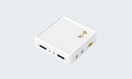
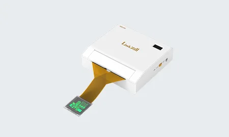
Built around TFT semiconductor technology, LinkZill’s platform covers material integration, driving and readout system, packaging, and bonding. By handling these engineering layers, the company allows research teams to concentrate on material and device innovation.
LinkZill’s technologies have been used in more than 300 high-impact papers, including over 20 publications in the Nature and Science family journals. This broad academic adoption has helped establish a new benchmark for system-level validation.
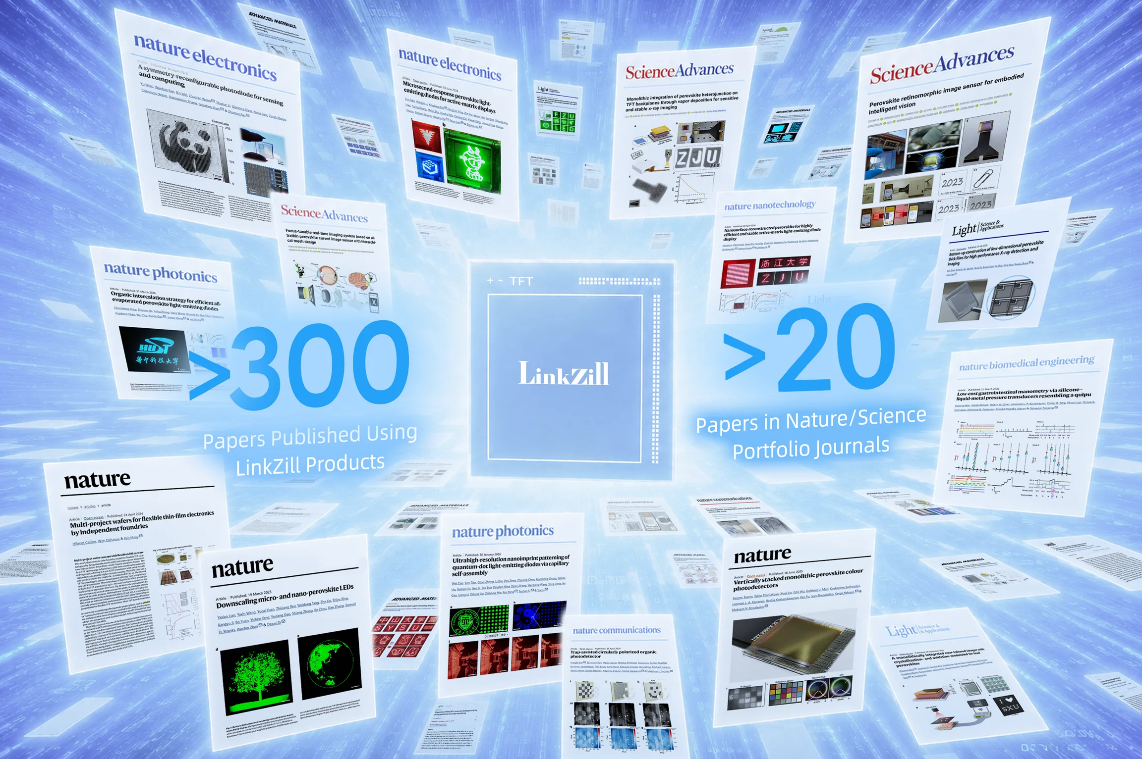
Several recent studies demonstrate the range of applications:
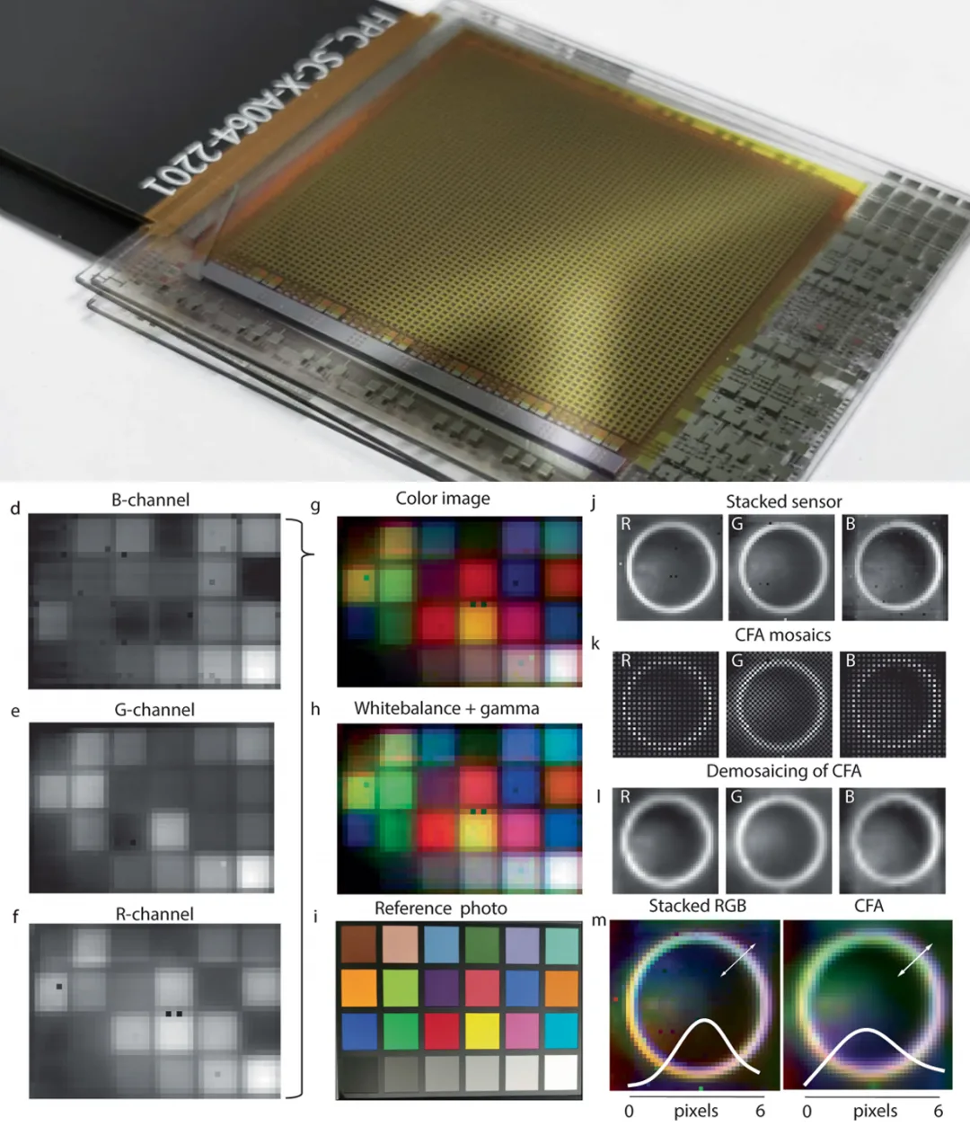
An ETH Zurich team integrated a novel imaging device with LinkZill’s TFT sensing chip. The resulting system enabled high-speed, multichannel signal readout and produced accurate, artifact-free color images without conventional filters or complex reconstruction algorithms.
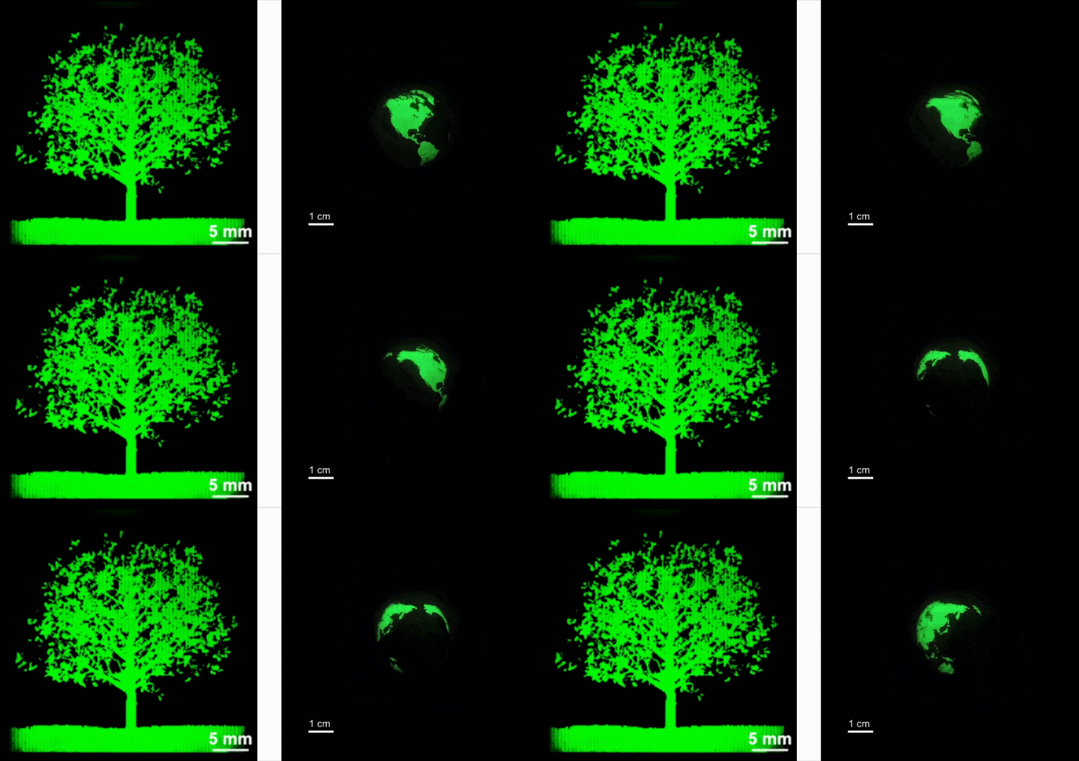
Researchers at Zhejiang University developed what they described as the world’s smallest LED. Working with LinkZill, they also produced an active-matrix PeLED micro-display prototype, pointing toward ultra-high-resolution wearable displays.
A joint team from Shanghai Jiao Tong University, Hefei University of Technology, and KAIST used TFT arrays to build a large-scale retinal neuromorphic computing system. Published in Science Advances, the system performs adaptive imaging under low-light conditions and completes the loop from sensing to decision-making directly at the sensor.
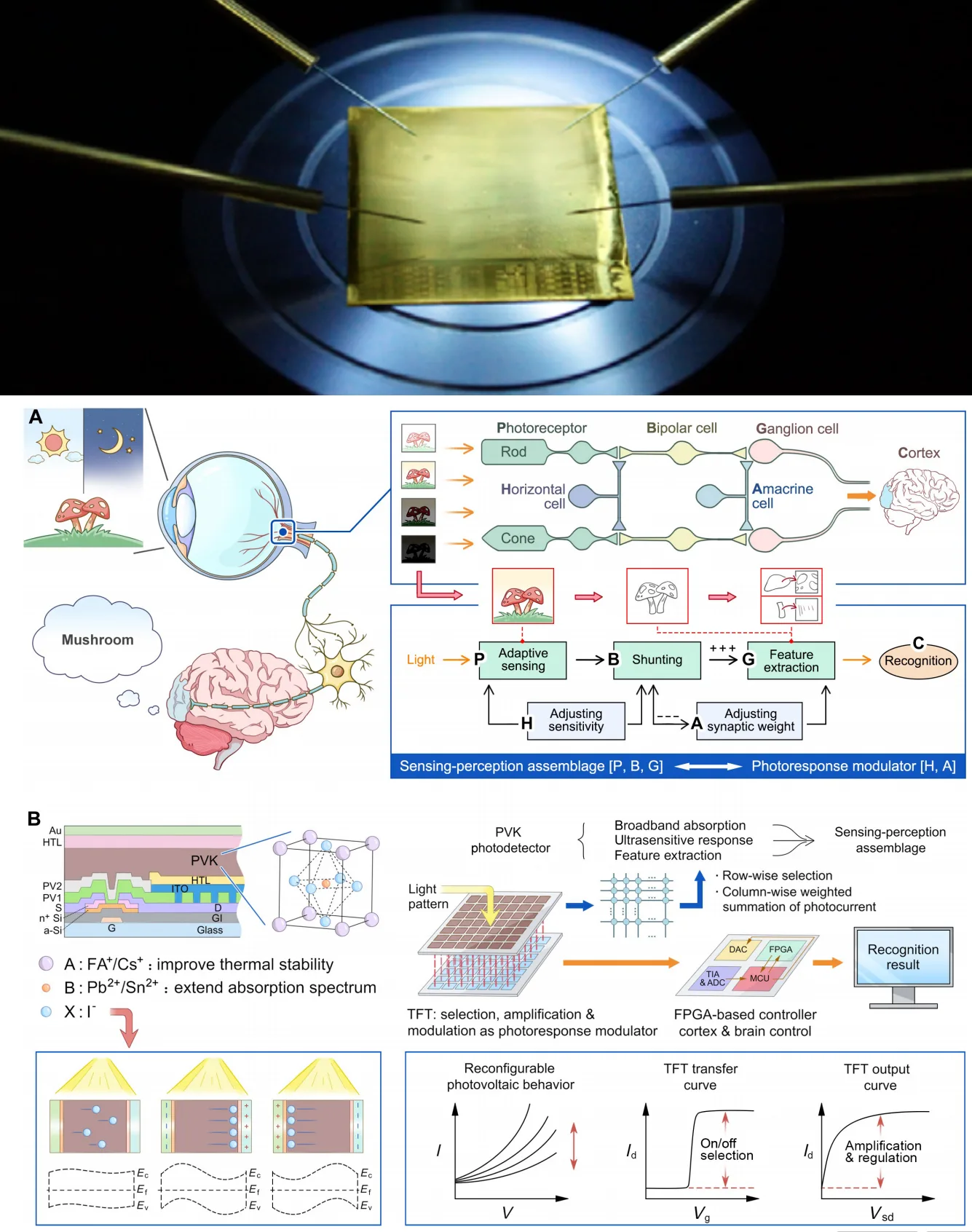
Together, these projects show that TFT platforms can support system-level validation across sensing, display, edge computing, and integrated sensing–memory–computing applications.
Bridging the Gap Between Laboratory and Industry
Laboratory validation, however, does not guarantee industrial readiness.
In May 2025, the U.S. National Renewable Energy Laboratory convened more than 50 experts in materials science, AI, and robotics to discuss how AI-driven discoveries could be translated into commercial products. Their central conclusion was that the “Valley of Death” between laboratory research and industrial deployment remains one of the barriers to commercialization.
Many scientific breakthroughs stall not because the underlying science is incomplete, but because converting a material into a product requires a long and costly engineering process.
Manufacturability is the first challenge. Research teams and early-stage companies generally need small production runs and repeated iterations. Using mature manufacturing lines for this work can be expensive, slow, and inefficient.
System integration is another barrier. Turning a material into a functional product requires circuit design, foundry processes, driving and readout electronics, packaging, and module assembly. Early-stage teams rarely possess all these capabilities in-house.
A reusable and scalable engineering platform is therefore essential for moving from published research to prototypes, pilot production, and ultimately commercial manufacturing.
This is the gap LinkZill aims to fill. The company has worked with more than 20 businesses across Europe, North America, and Asia in fields including next-generation displays, optoelectronic imaging, machine vision, electronic skin, and neuroelectronics. Its services extend from research validation and pilot trials to production engineering and mass manufacturing.
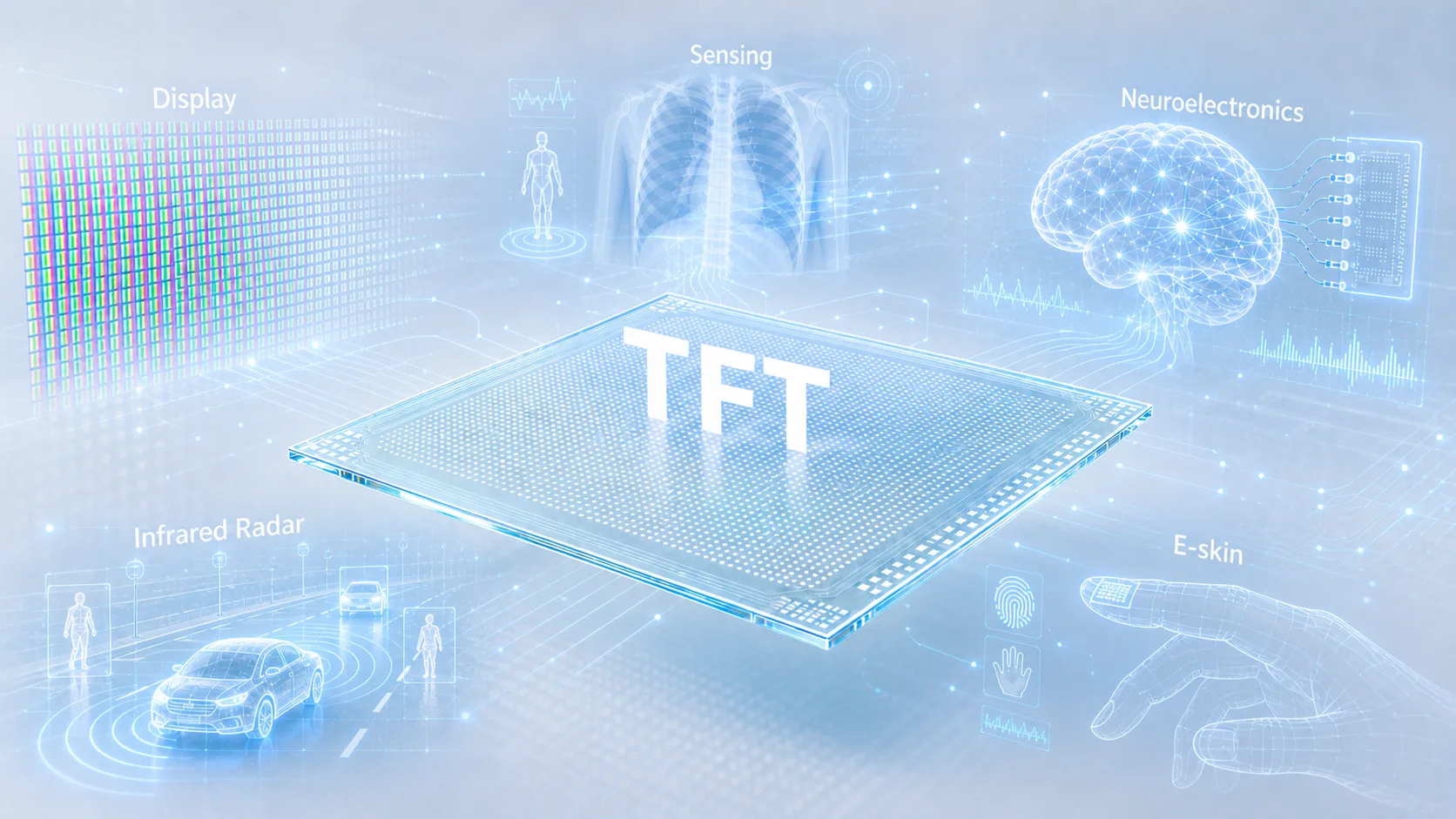
Rather than supplying TFT chips, LinkZill also provides driving and readout systems, along with application-specific prototype development. These prototypes allow early-stage companies to demonstrate more clearly how their technologies could become commercial products.
At the pilot stage, a European company used LinkZill’s TFT technology to develop an ultra-thin flexible OLED display for packaging and wearable applications. The project has secured more than US$10 million in funding.
At the pilot-production stage, LinkZill co-developed a flexible TFT inspection system with a UK startup. The product has entered commercial deployment and can cover larger areas and adapt to more complex environments than conventional inspection equipment, creating opportunities in aerospace, energy infrastructure, and smart manufacturing.
At the mass-production stage, LinkZill is working with a publicly listed European company on quantum-dot light-emitting materials for next-generation displays, with the goal of advancing the technology toward large-scale manufacturing.
Advancing the Next Phase of AI4S
LinkZill is headquartered in Hangzhou, with R&D centers and subsidiaries in Cambridge and Hong Kong. Its network spans more than 20 countries and regions, serving nearly 400 universities, research institutions, and technology companies.
The company was also identified as a representative player in TFT innovation in the Nature research article “Multi-project wafers for flexible thin-film electronics by independent foundries.”
Investor interest is growing as well. In 2026, semiconductor-focused investment firm Walden International invested in LinkZill. The company’s other investors include Supergravity Capital, ZhenFund, Apricot Capital, and Proxima Venture.
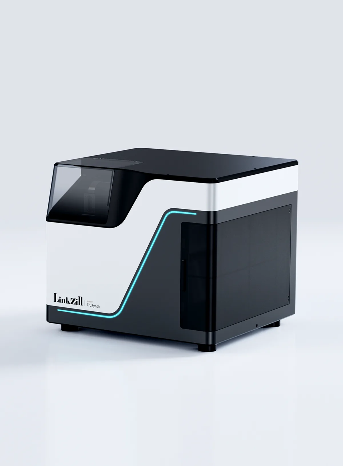
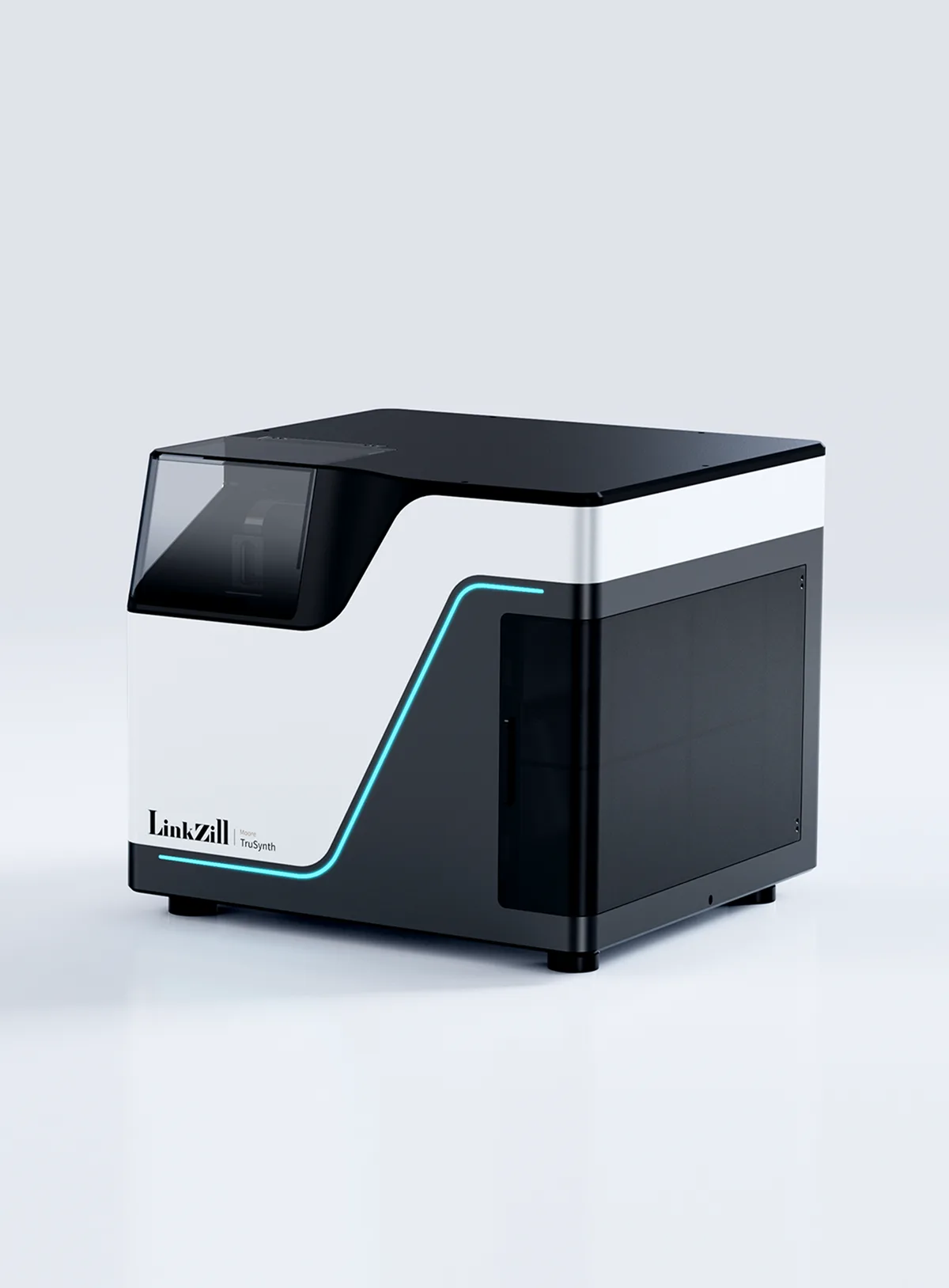
LinkZill is now extending its TFT platform into the life sciences. It has launched a benchtop oligonucleotide microarray synthesizer designed to improve the efficiency and reduce the cost of biological data generation through TFT-based DNA synthesis.
The underlying challenge is the same in both life sciences and materials research: as AI becomes better at generating hypotheses, screening candidates, and discovering new materials, the scarce resource is shifting from ideas to high-throughput, low-cost, and scalable validation.
TFT technology is therefore emerging as an important bridge between AI-driven discovery and industrial application—and LinkZill is positioning itself at a critical point along that path.