What is Thin-Film Transistor?
Thin-Film Transistor (TFT) is a semiconductor technology widely used in the display field,
including smartphones, large-size TVs, and laptops.
LinkZill builds a complete capability system spanning design, fabrication, and product development with the core technology of TFT semiconductor.
LinkZill builds a complete capability system spanning design, fabrication, and product development with the core technology of TFT semiconductor.
Core TFT Design Capabilities
LinkZill offers comprehensive device- to system-level design capabilities in TFT technology.

Device Physical Modeling and Optimization
Leveraging deep expertise in TFT device physics, LinkZill conducts precise modeling and optimization of device structures, material properties, and performance parameters.
Complex Functional Circuit Architecture Design
LinkZill designs and implements highly integrated, high-performance customized circuit architectures for specific applications. These include pixel addressing, driving, and compensation circuits, precision timing controlling circuits, gate driver circuits (GOA), multiplexers (DEMUX), and other key modules.
High-Precision Layout Design and Simulation Verification
Using advanced EDA tools, LinkZill develops high-density, high-reliability layouts and verifies their performance through electrical simulations, including timing, power consumption, and signal integrity.
Design Rule Checks and Manufacturing File Generation
Comprehensive DRC, ERC, and LVS checks ensure process compliance, and accurate lithography MASK files (e.g., GDSII) are generated for manufacturing.
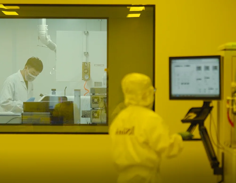
TFT Micro/Nano Fabrication Capabilities
Leveraging a self-operated 6-inch (compatible with smaller size substrates) micro/nano fabrication line and a semi-automated module backend line, supported by comprehensive utilities, EHS, and 6S systems, LinkZill has established and validated a wide range of processes on core micro/nano manufacturing and module integration.
Integrated Micro/Nano Fabrication Lines
Leveraging a self-operated 6-inch (compatible with smaller size substrates) micro/nano fabrication line and a semi-automated module backend line, supported by comprehensive utilities, EHS, and 6S systems, LinkZill has established and validated a wide range of processes on core micro/nano manufacturing and module integration.
High-Precision Front-End Processing
Capabilities include sub-micron to micron-resolution lithography and patterning, thin-film deposition such as sputtering for high-quality, thickness、uniformity-controlled metal and dielectric films, wet etching and lift-off processes for precious metal metal (e.g., Au, Pt) electrode patterning. Expertise also extends to micro/nano fabrication, surface treatment, and productization on flexible substrates such as polyimide (PI).
Back-End Packaging and Heterogeneous Integration
Supports flexible circuits printing, high-precision rigid chip dicing, and reliable flexible interconnect bonding (e.g., ACF/ACP lamination).
Process Control and Monitoring
Implement stringent online process monitoring, including thin-film transistor (TFT) layer thickness measurement, critical dimension (CD) controlling, and electrical performance (EP) testing, to ensure process stability and parameter consistency.
Small-Batch Manufacturing and Validation
Provides small-batch, multi-variety fabrication of micro/nano devices and modules, including prototyping, functional testing, and performance/reliability evaluation, ensuring stable, repeatable, and safe production.
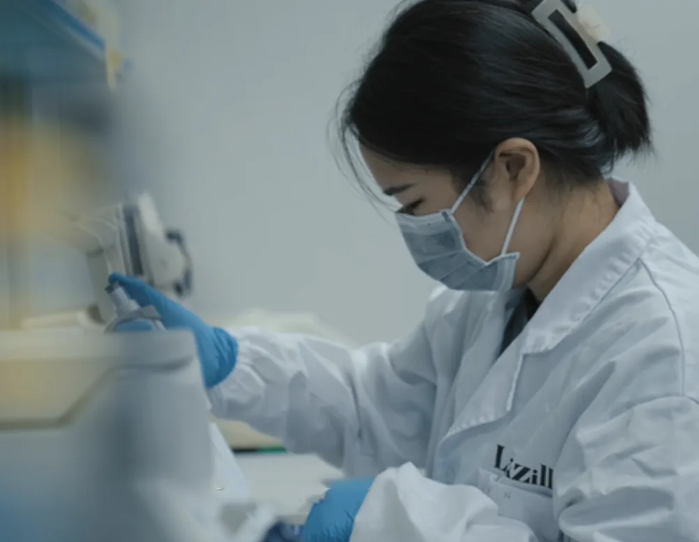
Macromolecular Chemistry, Surface Chemistry, and Electrochemistry
LinkZill has established a systematic capability spanning from macromolecular design and surface chemistry to electrochemical reaction driving and electrochemical signal sensing, providing a solid foundation for the R&D and application of high-performance life science chips.

- Precision drive capacity of electrochemical reactions on microarrays
- Design of electrochemical reaction systems
- Surface chemistry for chips and solid-phase carriers
- Macromolecular design for surface modification
- Hydrophilic/hydrophobic surface engineering of chip surfaces
- Chemical synthesis of natural and non-natural nucleic acids
- Microarray electrochemical signal sensing
- Electrochemically driven enzymatic reaction control
Biotechnology and Life Science Application Development
LinkZill has built comprehensive expertise in molecular biotechnology, high-throughput omics technologies, and bioinformatics, providing a strong foundation for robust quality control of high-throughput nucleic acid synthesis products, application development of oligo pools and microarrays, and the advancement of TFT-based life science devices.
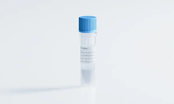
- High-throughput oligonucleotide products quality control system
- Library preparation, sequencing, and bioinformatics workflows for oligo pools and derivatives
- Sequence design for oligo pools and microarrays
- Solid-phase and liquid-phase capture
- Chip-based genotyping
- Fluorescent and electrochemical molecular labeling and detection
- Enzymatic reactions on chips and solid-phase carriers
- Reaction control in digital microfluidic systems
Electronic Engineering Capabilities
LinkZill delivers comprehensive in-house development across the full electronic system lifecycle, covering architecture design, hardware implementation, embedded system development, software integration, and system-level verification.

Full-Cycle Electronic System Development
• System-level architecture design
• High-reliability hardware development
• Embedded system development
• Testing and verification frameworks
Core Circuit Design Expertise
• Ultra-high precision signal chains
• High-speed data acquisiton
• High-speed data interfaces
• High-density analog front-ends
Leveraging its TFT design, fabrication, and development capabilities,
LinkZill has brought a diverse range of TFT applications to life.
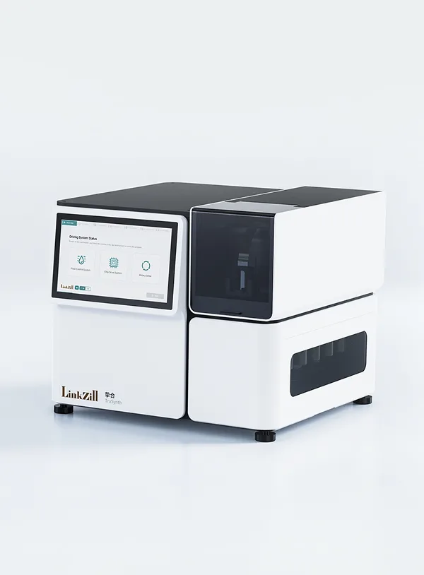
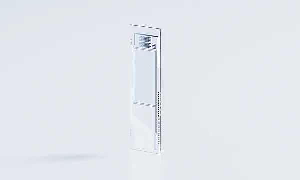
It encompasses TFT-based oligonucleotide synthesis chips, biosensing and detection chips,
integrated microfluidic chip systems, optoelectronic imaging chips (e.g., X-ray detectors), optoelectronic sensing chips,
smart IoT (AIoT) sensor node components, and bionic electronic devices.
TFT semiconductors are poised to power emergent AI-driven designs,
becoming the next-generation tools for life sciences.